Chapter 2
ExperimentSeveral steps are required for the determination of surface structure. The following sections describe procedure used for general surface structure-determination using LEED. Described in reverse order, they are the preparation of samples (using standard UHV practices), the determination of sample cleanliness (using AES), and the determination of surface structure (using LEED).
2.1 Low-Energy Electron Diffraction2.1.1 The Basics
LEED is the oldest surface science
technique [23],[24] and
is used to study the structure of
crystalline surfaces [25],[26].
From the acronym we can gather that the surface is probed
by low-energy electrons, and diffraction techniques give
us structural information.
Low-energy electrons,
with incident energy from 30 to 300 eV,
have wavelengths on the order of one Angstrom,
as given by the well known de Broglie relationship: 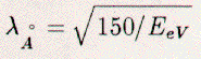 where λ is the electron wavelength (in Angstroms); E is the electron's energy (in eV). These wavelengths are comparable to the spacing between atoms both parallel and perpendicular to a crystal surface, hence, the electrons may diffract (elastically back-scatter) from the surface atoms. Since the cross section for scattering of low-energy electrons is very large, an incident electron beam attenuates within the top few surface-layers. The back-scattering is also strongly dependent on the type of atoms. LEED is, therefore, sensitive to the structure of surfaces. Kinematical diffraction theory, which is based on the approximation of single scattering and works acceptably for high-energy electrons and X-rays, cannot be used in the description of LEED. Instead, the complicated theory of multiple scattering must be used, which adds significant complication to the analysis. Nevertheless, some information about the surface can be gained from LEED before multiple-scattering theory is invoked. LEED can directly give information about the symmetry and in-plane spacing of atoms in a surface. A surface layer on a crystal can be described as a two-dimensional net of atoms. From this net, a reciprocal lattice can be constructed. Diffraction of electrons, elastic scattering by the surface, happens when momentum parallel to the surface is conserved between incoming and outgoing beams, up to the addition or subtraction of a reciprocal lattice-vector. These diffracted beams are indexed (hk) by the reciprocal lattice-rod from which they diffract. The outgoing beams are therefore a map of the surface reciprocal-lattice and display its symmetry.
Experimentally, see Figure 2.1,
a well-collimated monoenergetic beam of electrons,
created by an electron gun (EG),
impinges on a clean sample surface, usually at normal incidence.
Outgoing elastic
beams arise governed by the grating equation: 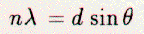 where n is the order of diffraction; d is an in-plane lattice distance; theta is the diffraction angle, measured from the surface normal, of the backscattered electrons. The diffracted electrons radiate out from the sample toward a display detector. This detector has four concentric hemispherical grids and an outer phosphor screen; The first grid, fourth grid, and sample are at ground potential. The second and third grids are at a potential several volts less than the electron-beam voltage. The screen is held at several thousand positive volts. Diffracted beams travel from the sample toward the detector's first grid through a field-free region. The next two grids filter out most inelastically scattered electrons emanating from the sample. The beams then travel through the fourth grid and are accelerated toward the screen. Beams appear on the hemispherical screen as fluorescing spots, and the arrangement of beam spots is called a pattern. This pattern caused by diffraction is an image of the surface reciprocal-lattice. As an example, Figure 2.2 is a schematic LEED pattern for the (111)1x1 surface at normal incidence. These beams are called the ``integral-order'' beams and arise from scattering from the bulk-like surface planes. The 3-fold rotation and mirror-plane symmetries of the surface creates degenerate beam-sets (10,0-1,-11), (01,-10,1-1), (11,-12,-21,-1-1,1-2,2-1) etc..... Figure 2.3 is a schematic LEED pattern from a Si(111)√3x√3-30-X surface. In this picture, the bulk-like and the superstructure reciprocal lattice-meshes are indicated. The additional beams, so called ``fractional-order'' beams, are labeled with respect to the integral-order mesh. Thus, the set of beams (a,b,c,d, e and f) is labeled (1/3 1/3, 2/3 2/3, 1/3 4/3, 4/3 1/3, 2/3 5/3, 5/3 2/3, respectively. Figure 2.4 is an actual pattern for the (111)7x7 clean surface. The 3-fold rotation and mirror symmetries are obvious. From the LEED pattern, we can gain information on the symmetry, surface unit-cell dimensions, and quality of the surface layers. Visual inspection of a pattern's symmetry can tell us the symmetry of the surface layer. Measurements of the diffraction angle (theta) can be made, from which the surface in-plane lattice spacing (d) can be determined. The presence of large regions with well-ordered surface structures can be deduced, though this is highly subjective, from the sharpness (size) of the beams and from the existence of only one pattern type. This is the use most researchers have found for LEED; there is, however, more information that can be obtained from LEED patterns. As an electron's energy increases its wavelength and the diffraction angle decreases and vice versa; therefore, with increasing energy the beams move toward the specularly-reflected electron beam. Patterns not only compress with increasing energy, but the intensities of discrete beams are modulated. If single scattering and infinite penetration were exactly applicable, then the beams would only have intensity at discrete energies. If single scattering in only one layer was exactly applicable, then the beams would have constant intensity for all energies. However, this is not so, and the intensity modulation is a result of multiple scattering within the top few atomic layers. The variation in the intensities of beams as a function of energy is a fingerprint of the surface structure. Hence, it is necessary to collect spectra of each beam's intensity as a function its energy (I-V curves) in order to characterize the surface. The spectra, however, cannot be Fourier transformed to reveal the atomic locations on the surface. Kinematical analyses have been tried, but generally yield incomplete or erroneous results. As stated earlier, multiple-scattering theory must be used to explain the spectra. A model surface-structure is first proposed, with which computer calculations (applying multiple-scattering theory) then produce theoretical I-V spectra, which are then compared to the experimental spectra. Usually, the model needs to have several structural and non-structural parameters systematically varied in order to minimize the differences between calculated and experimental spectra; this is the process of refinement. For example, the spacing between the surface planes is a structural parameter which needs to varied about the bulk inter-planar spacing in order to minimize the differences between calculated and experimental spectra. The optical-potential, which attenuates the electrons, and the Debye temperature of the model surface are two non-structural parameters that are varied to get the ``best-fit'' between calculated and experimental spectra. The evaluation of the fit can be accomplished both visually and numerically; the latter technique is similar to R-factor structure searches used in X-ray diffraction analysis. The surface structure is finally determined when the set of theoretical and experimental curves ``match.'' In this manner, LEED has been very useful in analyzing structures of surfaces which have been altered from their ``ideal'' bulk terminations. Described in the next sections are the general actions taken for the determination and preparation of Si(111)√3x√3-30-B, -Mg, -Au, and -Ce surface phases. 2.1.2 Data CollectionTo analyze the surface structure, experimental LEED I(V) spectra needed to be collected. Once the surface was prepared and a pattern was visualized, the sample was placed in the well-defined diffraction-condition of normal incidence. Such was done so in order to know that the incident angle of the incoming electron beam was zero. This angle was maintained throughout the range of electron energies by not moving the sample. Also, the residual magnetic field was eliminated around the sample with the introduction of Helmholtz coils which counteracted the Earth's magnetic field and stray fields from the surrounding apparatus. Thus, the incident and diffracted beams were not magnetically deflected, which would have altered the diffraction conditions. The integrated intensity of each diffraction beam can be measured in a variety of ways, the oldest of which is the Faraday box, which has also the advantage of measuring absolute intensities. The Faraday box must be made to follow the particular diffracted beam under scrutiny and the measuring process can be quite time consuming. A more rapid way to collect spectra implementing a video system was used for our research. The LEED pattern was viewed by a sensitive video camera. This camera was connected to a micro-computer which digitizes individual pixels in a video frame, see Figure 2.5 [27]. A microcomputer program took as its input the size and orientation of the surface net and calculated the corresponding reciprocal net. The matching of the observed pattern with the computer-generated mesh uniquely determined the diffraction conditions for all incident-electron energies. The computer then collected a single I(V) spectral-point by integrating the intensity of a LEED beam, i.e., by summing the digitized pixels within a video window which covered the individual spot. The computer did this process for all selected beams at a given energy, and scanned through all selected energies to create an I(V) spectrum for each beam. The scanning of the energy was done several times so as to increase the signal-to-noise ratio of the collected data; typically the spectra were scanned twenty times to garner counts in the range of 60,000. As many I(V) spectra as possible were collected, and the collection of degenerate spectra was useful in order to test for normal incidence. After a full set of spectra was collected, the data needed to be processed. First, the spectra were cropped to ensure that the beams were wholly on the screen of the LEED detector and were not shadowed by the edges of the screen as they emerged onto the screen. Second, degenerate beams were averaged to increase the signal-to-noise level and reduce the effects of slight non-normal incidence. Third, the beams were normalized to a constant incident electron-beam current by dividing out the incident-current spectrum, as measured on the sample. Fourth, the experimental background in each spectra was removed so as to place the minima of the spectra on the zero of the ordinate axis. This background subtraction process removed unwanted beam-intensity created by inelastic scattering and surface disorder. Finally, smooth spectra were created using convoluted Gaussian-filters and cubic-spline interpolation. The above processing was required so as to bring the experimental spectra into the realm of the ideal spectra as created by theoretical calculations. It can not be overstated that the degree of agreement between experimental and theoretical spectra depended heavily on the quality of the experimental spectra. The correspondence between theoretical and experimental spectra was evaluated both by eye and computationally by using R-factors. The eye could ``neglect'' relative peak-height differences, a monotonically increasing background, and noise; R-factors were, however, not so ``forgiving.'' Also, a larger data set (finer energy increment, larger energy range, and/or more beams) allowed for a more reliable structural solution. One or two spectra covering a range of 100 eV (with 5 eV steps) were insufficient. Five spectra, over 200 eV (with 1 eV steps), were usually sufficient. Ten or more beams were highly desirable. 2.1.3 AnalysisAs we have mentioned above, in order to determine structure using LEED, theoretical spectra were calculated. The details of such calculations are well documented in the literature [23]. We describe below the basic principles behind the Van Hove and Tong programs with layer-doubling used by Y.S. Tong and H. Huang to calculate the I(V) spectra for boron on Si(111). There exist other programs developed by J. Pendry (using renormalized forward scattering), W. Moritz, D. Jepsen (using the combined-space method), and others not described here, and we used the Jepsen's CHANGE program to calculate the I(V) spectra for gold on Si{111}. Prior to any I(V) calculations, a plausible model-structure is proposed based upon available information, and the elastic multiple-scattering of an electron by an atom is described in terms of plane wave phase-shifts. The phase shifts determine how an incoming plane-wave of electrons is altered by the presence of an atom core. The computational steps are:
This process includes scattering information for all required beams and spherical-wave angular-momentum. It must be recalculated for each desired energy point in the spectra and in part recalculated for structural-parameter changes. To reduce computation time, the symmetry of the pattern is exploited so as to reduce the number of beams that need be retained, and the energy ranges may be reduced in order to decrease the number of phase shifts. Also, calculated spectra are often completed on a large energy increment and then interpolated to the energy increment of the experimental spectra. Theoretical I(V) curves are then compared to the experimental spectra. Such a process is complicated by the number of spectra, for each possible structure, that need to be considered. Non-reconstructed metal surfaces usually have only a few structural parameters that may be altered: the surface unit-cell dimensions are bulk-like and the first interlayer-spacing might relax slightly. In the calculations the first interlayer-spacing may be varied from -0.10 Ang. to +0.10 Ang. in increments of +0.025 Ang., ang the second interlayer-spacing may be similarly changed. These calculations produce 81 theoretical spectra which are compared to one experimental spectrum firstby eye, then by reliability factors, and then verified by eye. This process is done for all the individual beams for which experimental data exists. As an example, eleven non-degenerate LEED I(V)-spectra were collected from the clean unreconstructed-surface of Tb(11-20) at normal incidence [28]. Calculated spectra (not shown here) generally agreed with experimental spectra even if little or no first interlayer-spacing (d12) contraction was assumed. The analysis was furthered by calculating spectra for a surface unit-cell which had atoms symmetrically displaced (Delta X) from the surface glide-line. Visual inspection became problematic, as comparison of hundreds of curves could not be accomplished systematically. Hence, R-factors were used. A contour plot, see Figure 2.6, showed that the surface was contracted by 3% and surface atoms were displaced away from the glide line by 20%. It is in this manner that LEED has been able to solve the surface structure for scores of metal surfaces [29]. LEED has been more successful in determining unreconstructed metal surface-structures than semiconductor surface-structures. Semiconductor crystals usually have large surface unit-cells, reconstruction occurs in several atomic-layers, and relaxations also occur in these layers. Hence, dynamical LEED analysis was not always practical from a computational point of view. However, this technique is now increasingly used not only to categorize the symmetry of semiconducting surfaces, but also to determine their structure [13, 30, 31, 32] For example, a new generation of computer code, developed by S.Y. Tong and H. Huang, which relies on the symmetry of the surface in order to reduce the number of beams, was used to study the clean (111)7x7 surface, discussed in Chapter~1. Because of the large number of structural parameters that had to be varied in the dynamical analysis, optimization routines were included in the code to ``zero in'' on the best model. Si(111)√3x√3-30-X surfaces are structurally less complicated than a 7x7 surface, but still not as simple as a non-reconstructed fcc{001} surface. For example, a Si(111)√3x√3-30-X surface may have relaxation of bonds in the top two Si double-layers. Within each single layer there are usually two inequivalent atoms. These atoms may relax perpendicularly to the surface planes or radially toward the center of in-plane symmetry. Therefore, neglecting the adsorbate, the sqrt(3) surface may have several variable structure-parameters. If we consider the independent changing of each parameter several-times, then the total number of calculations per model could be many thousands. Clearly, better schemes are needed to reduce the structural searching process. Hence, R-factors are now becoming an integral part of the LEED calculations. For example, the structural parameters are automatically modified by the Tong and the Moritz programs to follow a path of steepest decent for a reduction of R-factor values.
LEED reliability-factors
were introduced to dynamical
analysis by Zanazzi and Jona
[33]. Additional R-factors
appeared which have broadened the basis of data comparison.
The two simplest such R-factors are: 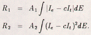
R1 is simply the integral of the absolute difference
between an
experimental (Ie) and a
theoretical (It) spectrum.
The two spectra are normalized to each other using the constant c
which is the ratio of the integrals of each spectrum, We and
Wt respectively.
The scaling constant for the R1 factor is just 1/We.
The R2 factor is just the integral of the squared difference
between the two spectra.
Similar simple R-factors
utilize the first and second derivatives of the
experimental and theoretical spectra or
the fraction of the energy interval in which
the two spectra have opposing slopes.
The more complicated rZJ-factor combines several of the
above into one comprehensive term: 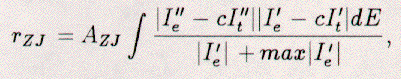 where the scaling constant, AZJ, is equal to 1/(0.027xWe). Other complex R-factors are a modified Zanazzi-Jona factor and the logarithmic Pendry R-factor (RP) [34]. Ten factors can also be combined to yield an average factor, RVHT, defined by Van Hove and Tong [35]. To date, most R-factor analysis is done with R2, rZJ, RP, and RVHT. The typical use of R-factors is as follows:
As stated earlier, semiconductor surfaces are more complicated than metal surfaces. With or without R-factors, the determination of the formers' structure can be daunting. Given two models (such as T44 or H3) for a Si(111)√3x√3-30-X surface, thousands of structures must be calculated for comparison with experimental spectra. There are, however, many other pitfalls, even if model A yields better agreement than model B, when comparing with the experiment. One, the experiment may not be ideal: an incorrect adsorbate-coverage, a mixing of various surface unit-cells, lack of normal-incidence, improper background-removal, a limited data set, surface contamination, etc.... can all yield I(V) spectra that are unknowingly unfit for comparison with theoretical spectra. Two, the calculations might be in error: the computer programs for I(V) calculations are often large black-boxes into which information (parameters) are blindly and sometimes erroneously passed. Three, the parameter space for model B might not be large enough to contain a solution with better agreement than for model A. Four, unconceived models may really be the true ``solution.'' Therefore, one model (for a given set of structural parameters) may be the lesser of two evils, but not the correct structure. LEED has been fortunate, however, is its ability to solve structures given good data, plausible models, computational efficiencies, insight from other surface techniques, and common sense.
2.2 Auger Electron SpectroscopyAuger-electron spectroscopy (AES) is the principal technique used to determine the concentration of elements on a surface [36]. When a surface is stimulated by high-energy electrons (3 keV) many interactions occur. It is possible that an incident high-energy electron ejects a core electron (e1) from an atom. A less-bound electron (e2) may then fall into the now-vacant core hole. This transition liberates energy (E1-E2) which may be emitted from the atom in the form of a photon. Alternatively, another less-bound electron (e3) may be ejected from the atom with kinetic energy equal to E1-E2-E3. This energy is highly elemental specific, since it depends upon three electron energy-levels of the atom. Of all of the elements in the periodic table, no two elements have the same set of electron energy-levels. Therefore, no two elements have the same set of Auger-electron transition energies. Typical Auger energies are in the range of 50 to 1500 eV. The mean-free paths of these electrons are in the range of 5 to 50 Angstrom. Hence, AES is a surface-sensitive technique, because Auger electrons emitted from a material must have originated in the near-surface region. Unfortunately, Auger electrons are not the only electrons emitted from a solid when probed by 3-KeV electrons. Most of the emitted electrons are inelastically-scattered electrons. A plot of the number of electrons emitted from the solid with a given kinetic energy, N(E), would display only a small peak at any particular Auger-electron transition energy. In order to enhance the detection of Auger-electron peaks, the spectrum of N(E) is differentiated. The experimental setup used in the present experiments is depicted in Figure 2.7, A beam of 3 KeV electrons was directed at the sample with a glancing angle of incidence. The glancing-incidence angle ensured that the incident beam probed mostly surface atoms and that the spatial cross section was large. Electrons emitted from the sample traveled toward the retarding field analyzer (RFA) in a field-free region between the grounded sample and the first grid of the detector. The analyzing voltage V (50 to 1500 VDC) and a small differential voltage (1 to 3 VAC, 1000 to 5000 Hz) were applied to the second and third grids. The fourth grid was again at ground and the screen (collector) was biased with a +300-VDC battery (B). At a given analyzing voltage, all emitted electrons with kinetic energy less than eV - eDeltaV could not reach the collector. All emitted electrons with kinetic energy greater than eV + eDeltaV entered the collector with a constant current. Electrons with energy within the window eV + eDeltaV were collected with an oscillating current. The output of the collector passed through a preamplifier (PA) which converted the current signal to a voltage signal, amplified and filtered the signal to a desired frequency range. The preamplifier output was connected to a Lock-In Amplifier, which also accepted the original oscillatory reference-signal. The Lock-In Amplifier removed the DC signal and detected only that part of the input signal that oscillated at the reference rate. This signal was the number of electrons with the analyzer energy. The amplifier could also detect only that voltage signal which was twice the reference oscillatory-rate. This output was N'(E), the derivative of N(E), ie, the Auger-electron spectrum.
A typical Auger spectrum, see Figure 2.8,
contains many peaks, which we compared to
standard spectra
[37].
The experimental spectrum shown in the figure,
for Au on Si(111), has silicon
peaks at 92 and 107 eV. A carbon impurity peak
is present at 272 eV, and the remaining peaks are from gold.
In specifying contamination levels we cite the ratio of
heights of the contaminant peak to the substrate peak.
For example, RC is equal to IC(272eV)/ISi(92eV).
Additionally, each element has a corresponding
sensitivity factors, see Table 2.1. Therefore, the atomic
concentration for each element (X) is written as: 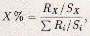 where the sum is over all elements (i) present on the surface under study. This formula is not accurate, assumes a uniform distribution of all impurity elements, and the standards were collected using a cylindrical-mirror analyzer, not an RFA. Nevertheless, AES gives us information on the cleanliness of a sample surface and the relative-concentration of contaminants.
Auger spectroscopy was also used to determine thicknesses
of deposited films.
To obtain coverages, we took into account the damping
of the AES signal by a layer of thickness d.
For example, in the case of Mg on Si, using the formula: 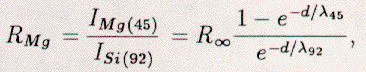 the thickness of the Mg film was approximated. This formula relies upon the exponential attenuation of the substrate signal (ISi(92)) in the denominator and the corresponding increase in the film signal (IMg(45)), when Mg is deposited on Si. R∞ is the ratio of intensities I∞Mg(45)/I∞Si(92) = 0.87 [z1]; I∞ is the intensity of the AES line for the semi-infinite element; the λ's are the inelastic mean free paths (IMFP's) for the AES electrons [38]; d is the thickness of the Mg film on the Si(111) surface; and uniform growth and material independent IMFP's (λ45 = 3.6 Ang., λ92 = 4.5 Ang.) [38] are assumed. The above equation could not be analytically inverted, however, to yield thickness (d) as a function of the ratio (RMg). Instead, it was parametrized and calculated for a range of possible thicknesses. Additionally, if the thickness of an atomic layer was known, then the thickness of the film was converted into coverage: monolayers (ml) if the film growth was layer-by-layer or layer equivalents (LE) if the growth mechanism was unknown. Often, however, the packing of the layer was unknown, interdiffusion may have been present, and the λ's may have been inadequate. Hence, experimentally-determined thickness values were often uncertain when determined with the above technique. In concluding this section, the thicknesses/coverages and the contamination levels determined with Auger-electron spectroscopy yielded approximately-correct though not highly accurate results.
2.3 Sample PreparationSurface-structure studies required obtaining, mounting, cleaning, and ordering the sample. In general, single crystals for most of the elements are available from specialty shops, at a cost. In the present experiments commercially-available silicon wafers were used as substrate samples. These wafers can be purchased cheaply, with a specific dopant and a specific resistivity, accurately oriented, and polished on one side. The wafers were only checked for orientation using Laue X-ray techniques and required no other metallographic handling. Before introduction into the sample chamber, a Si wafer was sized and etched. The etchant removed the thick oxide and any hydrocarbon `build-up;' the sample quickly formed a new, but thinner, oxide. The simplest such etchant was hydrofluoric acid (HF). More complicated techniques, such as the Shiraki method [39], preferentially left a very thin and passive oxide. Both techniques yielded generally the same result. The sample was mounted upon a commercially-available goniometer which allowed for the motion of the sample along three perpendicular-axes within a small volume (8 cm^3), for rotation of the sample about one axis in the sample plane (theta rotation), and for rotation about the surface normal (phi rotation). An additional tilt (psi) was possible; this yielded an effective rotation about the third axis, but the sample was also translated, i.e., tilt was not an independent motion. The sample holder also allowed for the heating of the sample to above 1400 C and cooling to -100 C. The former was accomplished using a tungsten filament mounted behind the sample; either electron-bombardment or radiation heating of the sample was possible. Cooling of the sample was possible via an electrically insulated stainless-steel U-tube and copper-braid attached to the front plate of the sample holder. The electrical isolation of the cooling mechanism allowed for the biasing, the floating, or the selective grounding of the sample. Special attention was given so that no materials were mounted forward of the sample's surface, because we did not want contaminants to be sputtered onto the sample's surface. Once the sample was mounted, the holder was introduced into the vacuum system, see Figure 2.9. The experimental chamber was a large stainless-steel 304 cylinder (18 in. diameter, 43 in tall) with many attached ports. Referring to Figure 2.9, the sample holder (SH) was attached to the top port, thus the sample's theta-axis was the cylinder's axis. Radial ports, at the same height as the sample's face, contained the detector (RFA) for LEED and AES analysis, the ion gun (IG) for sample cleaning, the electron gun (EG) for stimulating Auger electrons, a deposition source (DS) for adsorption studies, and various windows (W). The chamber also contained shutters, pressure gauges, and was connected to pumps, valves, etc.... After the sample holder was mounted into the chamber, the vacuum system was evacuated to a level of 1 millitorr, using adsorption pumps. An ion pump and a sublimation pump further decreased the pressure to approximately 1E-07 Torr. Subsequent heating (baking) of the chamber (10 hrs. at 150 C) hastened the desorption of gases from the chamber walls. Finally, an ultimate vacuum of 1E-10 Torr was typically achieved once the chamber was cool and all filaments were outgassed. With good vacuum achieved, cycles of cleaning began. The sample was first examined with AES. Then, the sample was cleaned by sputtering with argon ions. The ions had a typical energy of 375 eV, which allowed for a gentle ``sweeping'' of the surface without introducing large scale surface-defects. After a short bombardment (1 hour) the sample was checked again for cleanliness using AES. These cycles continued until an acceptable level of contamination was achieved, RC and RO being below 0.01. Next, the sample was annealed to restore the order removed by the cleaning process. The temperature of the sample was monitored using an infra-red detector (IRCON). Unfortunately, silicon was transparent to the infra-red light emanating from behind the sample. Hence, in order to avoid errors the sample temperature was often monitored with the infra-red detector focussed on the Ta or Mo sample-mounting foil in the immediate vicinity of the sample. The infra-red detector also yielded temperature measurements with larger error bars (plus-minus 50 C). The benefits of these detectors were, however, the ability to measure temperature from a distance. To reduce the error in the temperature measurement, a thermocouple could have been used instead of the IRCON instrument, but was undesirable during a experiment. This was because a thermocouple would have needed direct contact with the sample surface and its insulation could have caused charging effects. Be that as it may, the first anneal of a Si(111) surface (800 C, several minutes) usually yielded a well ordered Si(111)7x7 LEED pattern. Further anneal at higher temperatures (up to 1200 C) yielded better ordered patterns. The anneal process usually caused the accumulation of contaminants of the sample surface. In this case the sample had to be cleaned again. Subsequent anneal usually again caused contamination, but at a reduced level. Hence, several cycles of bombardment and anneal had to be required to achieve clean and well ordered surfaces. Once a good surface was prepared, adsorption studies began. The predominant technique for deposition, in the present experiment, was thermal evaporation. Specific details are mentioned in the following chapters. These chapters discuss the experimental work and analysis for boron, magnesium, gold, and cerium adsorbed on or in Si(111) surfaces.
|

