|
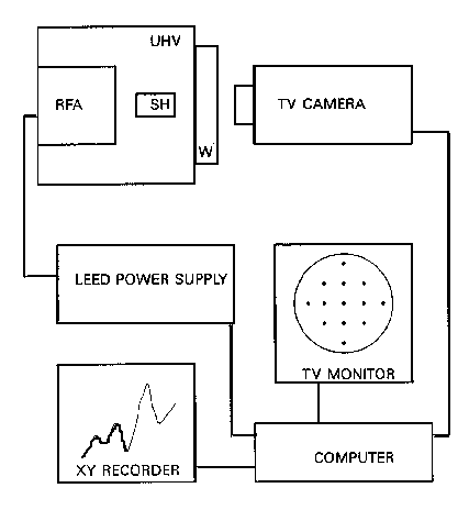
| Figure 2.5: Schematic LEED Data Acquisition System. The video camera views the diffraction pattern of the sample (SH) on the retarding-field analyzer (RFA) through the window (W) of the vaucum system (UHV). |

|
| Figure 2.5: Schematic LEED Data Acquisition System. The video camera views the diffraction pattern of the sample (SH) on the retarding-field analyzer (RFA) through the window (W) of the vaucum system (UHV). |
 Back to the experimental chapter