|
Chapter 3
B/Si{111}
AbstractThe past several years have seen many works on the Si{111}√3x√3-30-B system [40-65]. This is the last of the simple Si-group-III systems to be studied, probably because of its difficulty of preparation. Boron is a common dopant in p-type Si wafers, so Si{111}√3x√3-30-B promises to be a system of technological significance. Therefore, a dynamical LEED analysis of its surface has been completed and the structure has been determined. Boron atoms substitutionally occupy one third of the second-layer Si atom sites (B5) and the displaced Si atoms reside above in the T4-adatom locations. Attempts to produce an `all Si-rt3' surface epitaxially above the Si{111}√3x√3-30-B surface proved to be fruitless. Presented below are an introduction to the problem, a description of experimental details and analysis, and a discussion of the B5-Si{111}√3x√3-30-B relaxed structure and of the attempts to create new Si epitaxial structures. IntroductionThe formation of a Si{111}√3x√3-30-B surface has only been realized in the past few years. This was followed by a rapid search for its structure. Initially, models were proposed which involve 1/3 ml of boron in one of four different sites: T4, H3, B4, and B5. Hence, each model will be named after the boron-atom site, e.g., the T4-model involves a boron atom in the T4 site. RHEED studies [45] noted that as little as 0.2 ml of boron, deposited by the decomposition of HBO2 above 700 C, changed the 7x7 pattern to √3x√3-30: only Si and boron were present in the Auger-electron spectra. This structure was stable to anneal at high temperatures for long time periods. The T4-model was proposed for boron adsorption, considering the structure of the Si{111}√3x√3-30-Al, -Ga, and -In surfaces, see Appendix A. Korobstov et.al[44] prepared the √3x√3-30-B by anneal of highly-boron-doped Si crystals, noting that boron should segregate to the surface, as many contaminants often do [66,67]. On heating the Si{111}7x7 sample the LEED pattern changed from (7x7) to (1x1), then to √3x√3-30 after anneal to above 1000 C. Korobstov et.al. proposed the H3 site for boron. Note, cleaved samples with an initial 2x1 surface will also produce rt3 surfaces with high temperature anneal [47]. Thibaudau et.al.[46] prepared the √3x√3-30-B similarly to Korobstov [44]. They noted some asymmetry in the two halves of the rt3 unit-cell as visualized in the scanning tunneling microscopy (STM) images. A mirror-symmetry-breaking B4-model which involves Si-T4 adatoms at the corners of the unit cell and one substitutional boron atom in only one half of the unit cell was suggested. Bedrossian et.al.[42,51] prepared the √3x√3-30-B similarly to Korobstov[44], and Lyo et.al. [40,48,49] prepared the √3x√3-30-B by decomposing decaborane B10H14 on a Si{111}7x7 surface at 500 C. The occurrence of bright and dark atoms, imaged by STM, was noted. Increasing the boron concentration increased the number of dark atoms. Increasing the Si concentration increased the number of bright atoms. Therefore, boron was related to the dark atoms, but all the imaged atoms were believed to be Si. The lack of boron atoms on the top was confirmed by Lyo et.al.'s low-energy ion scattering (LEIS) results which only showed Si atoms on top. Further, the sites for both bright and dark atoms were confirmed to be T4 by comparing the registration of the rt3 mesh and neighboring 7x7 meshes on a low-coverage surface [42,51]. The dark atoms were identified as Si-T4 adatoms above a substitutional boron-B5 atom in the second layer. The low-concentration (15 to 20%) bright sites were thought to be defects involving the same Si adatoms, with no boron atoms substituted into the lower layer. STM spectroscopy above dark sites also revealed an unoccupied state associated with an empty Si dangling-bond and an occupied state associated with Si-Si back-bonding. Additionally, the symmetry in these STM spectra and topographic scans across the long diagonal of the rt3 unit-cell negated the B4-model. Total energy calculations (TEC) [40,42,43], concluded: a) that the B5-model was 1-eV more stable than both the T4-model and the B4-model for boron, and 2-eV more stable than the H3-model for boron, b) that the reduced bond length between B and Si in second and first layers, as compared to Si-Si, reduced surface stress, and c) that the Si-adatom dangling bond was removed by charge transfer to the accepting boron-B5 atom. Finally, an analysis using surface x-ray diffraction (SXD) [41] was the first direct attempt to verify the boron site selection. The boron-B5-model was proven to be correct, the other models were ruled out, and the surface was relaxed. Our own dynamical LEED analysis [30] came to the same conclusion independently from and simultaneously with the SXD study by Headrick et.al.[41] The atomic displacements found by LEED and SXD are within the mutually quoted errors. In the next section, the LEED experiment and the dynamical analysis will be presented. 3.2 Experiment3.2.1 Si{111}√3x√3-30-BHighly-boron-doped Si{111} samples, nominally 10x20x0.5 mm, p-type, 0.0016-0.0025 Ohm cm, and cleaved from a larger wafer were used for the experiment. Before being mounted on the goniometer, the samples were HF etched. The samples were then loosely mounted on a 0.025 mm-thick Ta disk, 25 mm in diameter, with care given so that no other materials were forward of the sample surface. This disk was then mounted on the goniometer which allows heating to 1400 C (e-beam bombardment), translation along three-perpendicular axis, rotation about two of those axes, and tilt about the third axis. Cleanliness and boron segregation were monitored with AES. Carbon and oxygen were the only detected contaminants. Particular attention was given to removing carbon since it might affect the surface structure. Several cycles of argon-ion bombardment (375 eV, 2.0 uA, 60 min., 5E-5 Torr, 30 C) followed by anneal at 1200 C for 20-30 min. reduced the contaminants to the noise level and segregated boron to the surface region. Typical values for the Auger ratios were, see Table 2.1, RC=0.002, RO=0.001, and RB=0.017. These ratios suggested much less than 1 at.% oxygen and carbon. Also, the contamination level did not increase even after overnight soaking in 1E-10 Torr vacuum. The above AES results are consistent with Lyo et.al.'s[49] finding that even NH3 at high dosages does not react with the passive top-layer of the Si{111}√3x√3-30-B surface. The boron ratio suggests a concentration of roughly 6 at.% boron, in agreement with other studies [44, 46, 47]. Although this boron concentration appears quite low, it does not suggest that the coverage is not 1/3 ml. The ideal coverage of 1/3 ml is defined as one adsorbate atom per three substrate atoms in the first layer. Several substrate layers contribute, however, to the AES spectra. We now know that within the top five layers there is one boron atom per thirteen Si atoms in the rt3 unit-cell. Neglecting lower bulk-layers, this implies a concentration of 8%. Furthermore, the boron is located below the surface layer, and the critical coverage for the formation of the Sirt3-B phase is small (other SXD results [62] state that only 0.07 ml of boron is necessary to reveal a rt3-B surface). The Si{111}√3x√3-30-B surface was prepared many times by anneal of the sample to temperatures between 1200 and 1300 C. Lower anneal temperatures of 1000 C only produced 7x7 patterns. Intermediate temperatures produced mixtures of both 7x7 and rt3 surfaces. When the rt3 surface was prepared, the LEED patterns were always very sharp, bright, and visible to high energies (>350 eV). Argon-ion bombardment would remove the surface order and the segregated boron; anneal to 1200 C would return the rt3 surface. LEED I(V) spectra were collected several times after several similar and different sample preparations. The spectra at normal incidence were always found to be the same, even if the sample had been soaking in the 1E-10 Torr vacuum for days. Non-normal incidence data were not collected because the large amount of data that could be collected at normal incidence was considered sufficient for a reliable intensity analysis. From a set of fifty-two LEED I(V) spectra, a final set of nine integral- and nine fractional-order spectra was created after averaging degenerate beams, normalizing to constant incident beam current, subtracting the background, and smoothing. These spectra (10, 01, 11, 20, 02, 21, 12, 30, 03, 1/3 1/3, 2/3 2/3, 4/3 1/3, 1/3 4/3, 4/3 4/3, 5/3 2/3, 2/3 5/3, 7/3 1/3, and 1/3 7/3 were used in the analysis to be discussed later. 3.2.2 Si/Si{111}√3x√3-30-BThe formation of an `all-Si rt3'surface was also attempted. Bedrossian et.al.[42] indicated that the rapid crystallization of epitaxial Si on a Si{111}√3x√3-30-B surface using solid-phase epitaxy causes the formation of a surface that has 80% bright adatoms. This surface was assigned to a subsurface-boron stabilization of the Si-rt3 overgrowth. Following Bedrossian et.al.'s recipe, Si was deposited by thermal evaporation onto a well ordered Si{111}√3x√3-30-B surface. Increasing amounts of Si gradually obscured the rt3 pattern and the boron AES signal was attenuated. The LEED pattern was completely obliterated by the deposition of 10 Ang. of silicon. Then the sample was heated to 1000 C for several seconds. This second step caused the appearance of sometimes either weak and fuzzy or bright and sharp rt3 LEED patterns. The spectra garnered from these patterns were, however, equal to those of the previously monitored B5-phase. The boron content, as determined by AES, also increased after the flash anneal. Attempts were also made using solid-phase epitaxy at lower temperatures. Progressive anneal (500, 550, 600 C etc....) of amorphous Si on a Si{111}√3x√3-30-B surface produced 1x1, 7x7, and rt3 patterns. These patterns often contained high background and diffuse beams. The spectra of these rt3 patterns were also equal to those previously collected from the B5-phase and the pattern remained unchanged after anneal to 1000 C. If the `all-Si rt3' could be created, then we would expect I(V) spectra different from the I(V) spectra of the B5-phase. Since the LEED spectra of all the rt3 surfaces prepared in this work were always the same, there was only one rt3-phase. The failure to produce an `all-Si rt3' surface was probably related to the continued segregation of boron atoms from the Si{111}√3x√3-30-B interface to the newly created Si overlayer's surface [44]. 3.3 LEED Intensity AnalysisDynamical LEED analysis for the determination of the Si{111}√3x√3-30-B surface structure was performed using models which correspond to 1/3 ml boron surface coverage in one of four different sites (T1, H3, T4, and B5). Within the analysis, the height of the atoms above the surface and the distances between atoms in the top four layers (two double-layers) were varied. Lower Si-layers maintained their bulk positions. Spectra for the above structures were calculated using a new generation of dynamical LEED computer code [13] which allows for the variation of many structural parameters by optimizing use of the C3v symmetry of the surface unit-cell and automated search using the Pendry reliability factor [34]. With such calculations, the T1- and H3-models could be ruled out as possible solutions of the Si{111}√3x√3-30-B structure. The B5- and T4-models produced lower reliability factors, with the optimized B5-structure yielding a reliability factor 25% lower than the next best T4-structure. The visual agreement between the spectra for the best calculated B5-structure and the experimental spectra was also noticeably better. The fractional beams were most sensitive to the structure of the rt3 surface unit-cell. Therefore, the greatest difference between calculated and experimental spectra occurred for the fractional-order spectra. The disparities might have been caused by the lack of a non-ideal experimental surface. The theoretical calculations assumed a 100% population of one type of unit cell across the sample face. However, the published STM data suggested that the surface was not homogeneous in structure; there were areas where almost 20% of the surface was thought to contain alternative rt3 unit cells involving Si adatoms on T4 sites without the underlying substitution of boron atoms in the second layer. Random defects alone would not markedly affect the location and relative intensities of peaks in the experimental LEED spectra. Different types of rt3 unit-cells would, however, change the spectra; averages of spectra from the different rt3 units would appear in the experimentally collected spectra. Thus, averaging of 80% of the optimized boron-B5 spectra and 20% of an `all Si rt3' (changing various structural parameters) was undertaken. The agreement between the newly averaged spectra and the experimental spectra did not improve. Other proportions (50/50, 20/80, 0/100) yielded equally poor results. Thus, we concluded that the all-boron B5-structure was correct. Surfaces prepared using the decomposition of boron compounds displayed more homogeneous and complete distribution of the boron-B5 surface unit-cell in the STM images [40,48,49]. Hence, LEED I(V) spectra of these surfaces are expected to be similar to those of the highly-boron-doped samples and closer to the calculations. The structural parameters for the relaxed B5-Si{111}√3x√3-30-B surface are listed in Tables 3.1 and 3.2, as found by the present LEED analysis, the Headrick et.al.'s[41] SXD study, total energy calculations [40], and a Keating energy analysis to be discussed later. The agreement between experimental and theoretical LEED I(V) spectra for Si{111}√3x√3-30-B can be judged in Figures 3.1, 2, 3, 4, 5, and 6. Corresponding reliability factors are listed in Table 3.3. The values of ½RP equalling 0.20 suggest acceptable levels of agreement, especially considering the large number of beams. The values of the reliability factors for the integral-order beams are low, as expected, since these beams contain mostly bulk information. The values of the reliability factors for the fractional-order beams are higher, as expected, since the B5-rt3 phase was probably not uniform across surface. The results of the three studies agree well within the quoted error margins. The differences may be due to the inability of the SXD work [41] to determine the actual placements of the boron atom in the substitutional B5 site and of the Si atom in the adatom T4-site: the bond length between the second-layer boron atom and the third-layer Si atom was fixed at 2.0 Ang. and no particular value of the Si-adatom height was quoted. Thus, the bond length between the Si adatom and the first-layer Si atom could not be determined. In the TEC study [40], the positions of only four atoms were quoted, but the results agree well with the results of the x-ray diffraction and electron-diffraction analyses. The main features of the structure involve the substitution of a boron atom for a Si atom in the second layer. The replaced Si atom then resides above the boron atom in the T4-adatom site. The boron atom relaxes 0.50 Ang. downward (toward the bulk), the lower Si atom relaxes 0.34 Ang. downward, the first-layer Si atoms relax 0.30 Ang. both radially toward the boron atom and downward, and the Si adatom resides 2.32 Ang. above the boron atom. In this configuration, the bond lengths between the Si adatom and first-layer Si atoms are 2.33 Ang., as opposed to the normal bulk 2.35 Ang. bonds. The boron-to-silicon bonds are 2.15 and 2.19 Ang. long, relatively close to the 2.06 Ang. value which is the sum of the tetrahedral covalent radii. The resultant surface has high stability as indicated by the apparent high heat of formation, its chemical inertness, and the nearly-ideal bond lengths. 3.4 Keating Energy Analysis
The stability of the B5-Si{111}√3x√3-30-B structure arises from
both electronic and elastic effects.
We have modeled the elastic effects by using
a Keating energy analysis [21].
The total Keating energy of the crystal
may be written as: 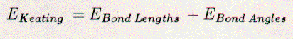 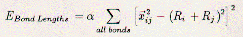 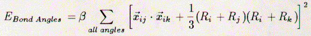 The vector xij is the interatomic vector between atoms i and j. Ri is the tetrahedral covalent radius of atom i. The scaling constants alpha and beta are 0.210 eV/Ang.4 and 0.0183 eV/Ang.4 [22], respectively. Thus, the Keating energy is an elastic energy sensitive to interatomic bond compression, expansion, and bending. The length term increases when an interatomic bond is larger or smaller than the sum of the radii. The angle term increases when the angle between bonds differs from 109.5 degrees. The scaling constant alpha is larger than beta. Hence, bonds may more easily be bent than relaxed. The starting place for the Keating analysis is an unrelaxed Si{111}1x1 surface, see Figure 3.7. The bulk terminated surface contains only atoms which are tetrahedrally coordinated with ideal both lengths of 2.35 Ang. The Keating energy for this surface is zero. Electronically, this is still a highly energetic surface due to the presence of the dangling bonds. Saturation of these bonds by an adsorbate on the T1 sites would also lead to a Keating energy of zero. This is because the bond between the adsorbate and a first-layer Si atom would become the sum of tetrahedral covalent radii and all Si-Si bonds would remain unchanged. The above model is, however, insufficient for our purposes, since it requires three adsorbate atoms per rt3 surface unit-cell to fully saturate the Si dangling-bonds. Instead, the H3-, T4-, and B5-models are the plausible structures. Referring to Figure 3.7, we see that one adsorbate atom per rt3 surface unit-cell can completely saturate the dangling bonds. There are, however, competing forces. First, the Si atoms want to maintain 109.5 degree bond-angles. Second, the adsorbate (X) and Si atoms must move to reduce the X-Si bond length to RX+RSi. Third, the displacements of the Si atoms must ebb as we approach the lower bulk-layers. We have modeled the H3-, T4-, and B5-models for the range of adsorbate radii from 0.78 to 1.58 Ang., in steps of 0.10 Ang. The tetrahedral covalent radii for C, B, Si, Ge, Al, Ga, Sn, In, and Pb are 0.77, 0.88, 1.18, 1.22, 1.26, 1.26, 1.40, 1.44, and 1.46 Ang. [66], respectively. In each case, the adsorbate atom and all atoms in the top two double-layers have been allowed to move. All atoms within the rt3 unit-cell may relax in the direction perpendicular to the Si{111} surface. Only some atoms may move radially toward the three-fold rotation axis, while maintaining the mirror symmetry of the unit cell. Each calculation (a given adsorbate and model) begins with the starting structure displayed in Figure 3.7. Then, all atoms are simultaneously moved in steps of 0.1 Ang. and the Keating energy is totalled. Once the minimum energy structure has been determined, the motions are reduced to steps of 0.05 Ang. and the process is repeated. This process stops when the motion step is below 0.001 Ang., and changes in the Keating energy are negligible. The H3-model reveals generally the lowest Keating energy for all adsorbates, see Figure 3.8. Although this model is elastically the most stable, it is not electronically the most stable and is not the structure determined for any of the 1/3 ml Si rt3-X surfaces with group-III or -IV adsorbates. This fact is clearly demonstrated by the distance between the adsorbate (Al or B) atom and second-layer Si atom (Si(2a)), see Tables 3.4 and 3.5 as well as Figures 3.9 and 3.10 The adsorbate (Al or B) is an acceptor, thus must be relatively near to the Si(2a) atom for charge transfer to be allowed. The T4-model allows this proximity and thus is preferred over the H3-model. Additionally, the structures determined for the H3-model of Si rt3-Al, -Ga, -Sn, and -Si using the Keating analysis are different from those determined by total energy calculations. This suggests that the Keating analysis starts with a structure that is inherently incorrect. The elastic energy analysis does not take into account electronic or chemical effects. Rehybridization, dangling bonds, lone pairs, and bond count are not modeled by our analysis. A plausible model with full tetrahedral (sp3) coordination is assumed. Therefore, it is not surprising that the H3-model yields misleading results. The B5-model reveals an even lower Keating energy for the Si{111}√3x√3-30-B surface than the T4-model. The failure of the T4-model may be attributed to the very small bond angle between bonds B(0)-Si(1) and Si(1)-Si(2a). The same angle for the B5-model is nearly ideal. Additionally, with decreasing covalent-radius (adsorbate size) many large motions of the substrate Si atoms are required for the T4-model, see Table 3. 6 and 3.7. These large motions of Si atoms create large stresses. The Si{111}√3x√3-30-B surface overcomes this by switching to a different structure, the B5, which requires less substrate relaxation. Additionally, the B5-model is electronically more stable than the T4-model, for boron, due to the five-fold coordination of the adsorbate. The Keating results agree well with the structures determined by LEED, SXD, and TEC analysis for the T4-Si{111}√3x√3-30-Al, -Ga, -Sn, and -Pb surfaces (see Appendices A and B) and for the B5-Si{111}√3x√3-30-B surface. For example, the parameters listed in column 2 of Table 3.4 for the T4 structure of Si{111}√3x√3-30-Al are the out-of-plane (Δz) and in-plane (Δr) displacements of the Al atoms in the top layer and Si atoms in the four lower-layers. The Keating energy analysis has determined the parameters ΔzAl(0), ΔzSi(1), ΔrSi(1), ΔzSi(2a), ΔzSi(2b), ΔzSi(3a), ΔzSi(3b), and ΔzSi(4a) to be +0.47, -0.04, -0.13, -0.31, +0.12, -0.30, +0.11, and +0.08 Ang., respectively, as compared to those same parameters determined by a dynamical LEED analysis [32] which are +0.62, +0.02, -0.15, -0.44, +0.16, -0.32, +0.08, and 0.00 Ang., respectively. In regard to the Si rt3-B, the structural parameters, see Table 3.1, from all four analyses (LEED, SXD, TEC, Keating) have the same direction of relaxation and order of magnitude. However, the Keating analysis requires changes of the atomic positions in lower Si layers that have not been found by the three other analyses. Without these changes the elastic energy is several percent larger. This fact is clearly demonstrated by the large Keating energy for the structures determined by LEED, SXD, and TEC analyses, see Table 3.2. The angle terms of the Keating energy for the four analyses are generally the same, but the bond terms differ greatly. These large energies arise from the deviation of B-Si and Si-Si bonds lengths from 2.055 and 2.35 Ang., respectively. A Keating analysis for the Ge{111}√3x√3-30-X surfaces also reveals the same trends as for the Si{111}√3x√3-30-X surfaces. First, the H3-model generally allows for the lowest elastic energy, see Figure 3.11. This model has not been confirmed for any of the Ge{111}√3x√3-X surfaces and it places the adsorbates in a chemically undesirable three-fold coordination. Thus, we exclude it from consideration. Second, the T4-model is energetically favorable for large-radius adsorbates and the B5-model is preferred for boron. Third, the results for Ge{111}√3x√3-30-Sn and -Pb agree well with the published experimental results [69], see Tables 3.8, 3.9, 3.10, and 3.11. Finally, even though there exists no experimental determination of the Ge{111}√3x√3-30-B surface structure, we feel confident that it would be the same as for Si{111}√3x√3-30-B. 3.5 Discussion3.5.1 Si{111}√3x√3-30-BAdditional surface science techniques have been applied by other researchers toward determining the structure of the Si{111}√3x√3-30-B surface. The dynamical LEED results are different from those of a recent LEIS study [63] which concluded that the structure would have 0.25 Ang. radial displacements and 0.1 Ang. perpendicular displacements of the Si atoms. Unfortunately, however, that study neglected the impact on the structure of a sub-surface boron atom and assumed that the top double-layer to be bulk-like. A photoemission and inverse photoemission study [43] resolved the predominant states in the valence band, which were identified as being an unoccupied state from an empty Si dangling-bond and an occupied state from Si-Si back bonding. These results are consistent with the boron-B5 structure. The substitutional boron atom displaces a Si atom to the T4 site. This Si adatom transfers charge to the accepting boron atom. An empty Si dangling-bond is created and the Si-adatom back-bonds to the first-layer Si atoms. The boron B5-structure is also consistent with core-level photoemission data [52], which showed a strong surface component of the Si 2p spectra. The strong Si 2p signal was related to the Si-B binding in the top double- and adatom-layers; this could not be explained with a boron T4-model, which would contain less Si atoms involved with boron. The polarization dependence of the boron 1s spectra also indicated a transition to a Si unoccupied-bond perpendicular to the plane of boron atoms. This indicated that the Si adatom was above the boron substitutional atom. The B5 solution is also consistent with a recent HREELS work which finds strong 59 meV and 107 meV vibrational losses [64]. The former is related to the strong back-bonding of the Si adatom to the first layer Si atoms, the latter, to the bonding between boron and Si atoms. This peak would have greatly reduced intensity had the boron atom been above the first double-layer and surrounded by fewer Si atoms. In conclusion, the group-III and -IV metals form 1/3 ml rt3 structures on the Si{111} surface. The small boron atom forms the B5 structure by substituting for a second-layer Si atom, which then resides above in an adatom position. The covalent radii of Al, Ga, In, Pb, and Sn are larger than the radius of boron. Therefore, they cannot substitute for Si atoms as the smaller boron atom does. They reside in the T4 site and create compressive stresses in the top Si layers. Hence, these surfaces are less stable than the Si rt3-B surface. Further, boron has been found to form Si{001}2x1-B [54] and GexSi1-x{111}√3x√3-30-B [62] stable structures. Although these structures have not been determined, they have been extensively studied for use as substrates for epitaxial Si over-growth. 3.5.2 Si{111}√3x√3-30-BThe attempts to form epitaxial overlayers were motivated by a desire: a) to form an `all-Si rt3' phase and determine its structure, and b) to study the epitaxy itself. In regard to the `all-Si rt3', the report of such a structure by Bedrossian et.al.[42] added to the debate about the Si{111}√3x√3-30-Ag, -Ta, and -Si surface structures. Bedrossian et.al. concluded the `all-Si rt3' surface to be a Si-T4-adatom structure created by the solid-phase epitaxy of Si stabilized by a sub-surface Si-rt3-B interface. This has not been reproduced by the present LEED work. The Si rt3-Ag, -Ta, and -Si surfaces were reported to be created by deposition (Ag,Ta) [70] on Si{111}7x7 or heat quenching (Si) [31] of a bombarded Si{111}7x7; these three surfaces had the same LEED spectra. Therefore, it was concluded, by Fan et.al.[31], that they were all the same impurity-stabilized structure, which was metastable in nature. This structure, which these authors determined by LEED analysis, involved a missing 1/3 ml of first-layer Si atoms. In would be interesting to compare the `all-Si rt3' phase of Bedrossian et.al. with the `all-Si rt3' phase of Fan et.al. If the two phases were the same, then the I(V) spectra would be the same. Unfortunately, since we failed to produce the Bedrossian et.al. `all-Si rt3' phase, the comparison could not be made. It must be noted, however, that other attempts to form the Fan et.al. `all-Si rt3' phase (quenched Si rt3-Si and deposited Si rt3-Ta surfaces) have also yielded mixed results [71,72,73,74]. Furthermore, our Keating energy analysis indicates that the relaxed Bedrossian et.al. `all-Si rt3' phase would be elastically less stable than a Si rt3-B phase, and the former still has one highly-energetic Si dangling-bond per √3x√3-30 unit-cell. Hence, if sufficient boron is present, then we expect the Si rt3-B phase to be dominant. In regard to Si epitaxy, initially deposited Si goes down amorphously and does not remove the Si rt3-B structure. This agrees with other studies [41,50] which indicate that the Si adatoms are removed by the deposited atoms, but the sub-surface boron is unaffected. These facts further support the B5-site selection for boron which is unperturbed by deposited Si atoms. These phenomena do not occur with the Si{111}√3x√3-30-Ga structure [53]; upon Si overlayer deposition the T4-Si rt3-Ga structure is immediately destroyed and Ga easily diffuses into the silicon. w Our results with Si solid-phase epitaxy are, however, contradictory with SXD data [50,75,76] that indicate the Si epitaxial film to be rotated by 180 degrees with respect to the bulk. If this was the case, the LEED spectra would display the same rotation. In other words, the 10 beam would become the 01 beam, etc.... The interchange of diffraction beams has not been noted in the present research and we cannot conclude that the overlayer/bulk interface is twinned. The solid-phase-epitaxy results are also different from those of chemical-vapor deposition [52,54], at lower reaction temperatures (500 C) can form epitaxial overlayers without segregating boron from the interface. This process allows for the preparation of boron-delta-doped layers deep within Si{111} crystals. On Si/SiP001}2x1-B, chemical-vapor deposition does not produce boron-delta-doped layers, but molecular-beam epitaxy does produce boron-delta-doped layers. In conclusion, boron can be placed in the surface of Si{111} by segregation from the bulk or by decomposition of boron compounds. In both cases, the Si{111} surface-structure changes from 7x7 to √3x√3-30, with boron atoms located in the B5 site. This is a substitutional site in the second layer of the surface with a Si adatom directly above, hence the smaller covalent radius of the boron atom allows surface stresses to be accommodated within the first few atomic layers, yielding a very stable structure. The formation of an `all-Si rt3' phase by solid-phase epitaxy on a Si-rt3-B surface could not be realized. Boron continued to segregate through the overlayer to the new surface. |

