|
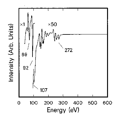
| Figure 2.8: Typical Auger-electron spectrum for Au deposited on Si{111}. The peaks as 92 and 107 eV are from silicon; the peak at 272 eV is from carbon contamination; and the remaining peaks are from gold. |

|
| Figure 2.8: Typical Auger-electron spectrum for Au deposited on Si{111}. The peaks as 92 and 107 eV are from silicon; the peak at 272 eV is from carbon contamination; and the remaining peaks are from gold. |
 Back to the experimental chapter