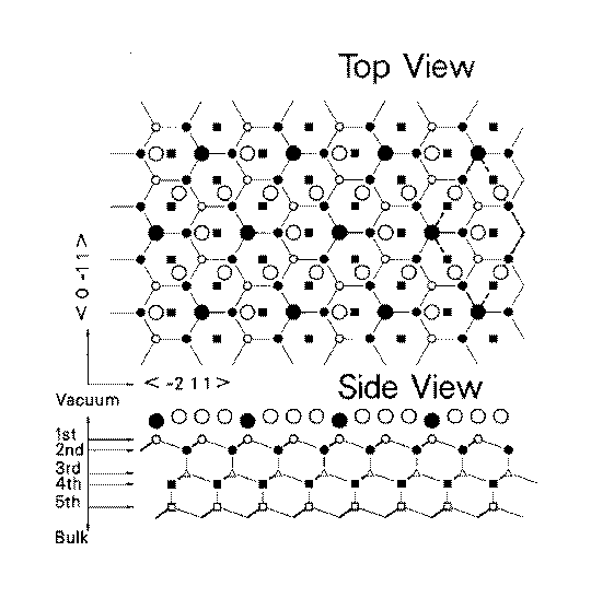
Figure 4.3:
The T_1^2 model for Si{111}rt3*rt3-30-Pb.
The Pb atoms form a close-packed layer centered on T_1 sites.

 Back to the List of Figures
- Figure 4.1: The T_4^2 model for Si{111}rt3*rt3-30-Mg. The Mg atoms form a close-packed layer centered on T_4 sites.
- Figure 4.2: The H_3^2 model for Ge{111}rt3*rt3-30-Pb.
- Figure 4.3: The T_1^2 model for Si{111}rt3*rt3-30-Pb.
- Figure 4.4: The H_3-T_4 model for Si{111}rt3*rt3-30-Au.
- Figure 4.5: The H_3-T_1 model for Si{111}rt3*rt3-30-Bi, -Sb, and -Au.
- Figure 4.6: The T_4-T_1 model for Si{111}rt3*rt3-30-Bi, -Sb, and -Au.
- Figure 4.7: Top: The superposition of schematic 1*1 (closed circles) and
Si{111}(2/3)rt3*(2/3)rt3-30-Mg (open circles) LEED patterns.
Bottom: Schematic top-view of the Si{111} surface. The large and small
circles are fist and second layer atoms.
The reciprocal and real
unit-meshes are indicated.
- Figure 4.8: Schematic LEED patterns for Si{111}3*3-Mg and 3*1-Mg.
- Figure 4.9 and
4.10: The I(V) spectra of Si{111}3*1-Ag, -Li, -Na, and -Mg.

